- 您现在的位置:买卖IC网 > Sheet目录509 > SI4420-D1-FT (Silicon Laboratories Inc)IC TXRX FSK 915MHZ 5.4V 16-TSSOP
�� �
�
�Si4420�
�RX-TX� ALIGNMENT� PROCEDURES�
�RX-TX� frequency� offset� can� be� caused� only� by� the� differences� in� the� actual� reference� frequency.� To� minimize� these� errors� it� is� suggested� to�
�use� the� same� crystal� type� and� the� same� PCB� layout� for� the� crystal� placement� on� the� RX� and� TX� PCBs.�
�To� verify� the� possible� RX-TX� offset� it� is� suggested� to� measure� the� CLK� output� of� both� chips� with� a� high� level� of� accuracy.� Do� not� measure� the�
�output� at� the� XTL� pin� since� the� measurement� process� itself� will� change� the� reference� frequency.� Since� the� carrier� frequencies� are� derived�
�from� the� reference� frequency,� having� identical� reference� frequencies� and� nominal� frequency� settings� at� the� TX� and� RX� side� there� should� be�
�no� offset� if� the� CLK� signals� have� identical� frequencies.�
�It� is� possible� to� monitor� the� actual� RX-TX� offset� using� the� AFC� status� report� included� in� the� status� byte� of� the� receiver.� By� reading� out� the�
�status� byte� from� the� receiver� the� actual� measured� offset� frequency� will� be� reported.� In� order� to� get� accurate� values� the� AFC� has� to� be�
�disabled� during� the� read� by� clearing� the� "en"� bit� in� the� AFC� Control� Command� (bit� 0).�
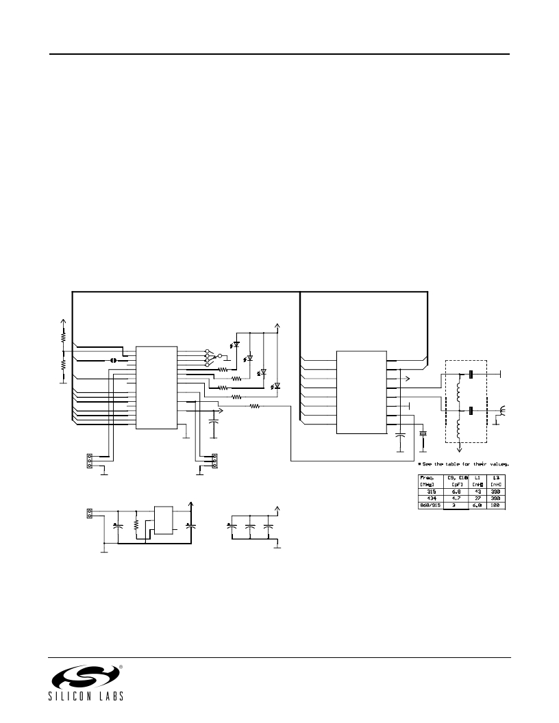
�TYPICAL� APPLICATIONS�
�Repeater� Demo� (915� MHz)�
�Schematics�
�GND�
�SEL�
�CLK�
�IRQ�
�SCK�
�MISO�
�MOSI�
�FFS�
�FFE�
�INT/VDI�
�ARSSI�
�SJ1�
�1�
�2�
�TX�
�RX�
�2�
�1�
�28�
�27�
�26�
�25�
�24�
�23�
�22�
�21�
�20�
�19�
�18�
�17�
�16�
�15�
�IC1�
�P0.0� P2.0�
�P0.1� P2.1�
�P0.2� P2.2�
�P0.3� P2.3�
�P0.4� P2.4�
�P0.5� P2.5�
�P0.6� P2.6�
�P0.7� P2.7�
�P1.0� P3.0/C2D�
�P1.1�
�P1.2� /RST/C2CK�
�P1.3�
�P1.4� VDD�
�P1.5�
�P1.6�
�P1.7� GND�
�C8051F311�
�14�
�13�
�12�
�11�
�10�
�9�
�8�
�7�
�6�
�5�
�4�
�3�
�1�
�4�
�3�
�6�
�SW1�
�5�
�R3� GND�
�820� R4�
�R5� 820�
�820� R6�
�820�
�VCC�
�C1�
�100nF�
�R7�
�1k�
�MOSI�
�SCK�
�SEL�
�MISO�
�IRQ�
�FFS�
�FFE�
�CLK�
�1�
�2�
�3�
�4�
�5�
�6�
�7�
�8�
�IC2�
�SDI� NINT/VDI�
�SCK� ARSSI�
�NSEL� VDD�
�SDO� RF1�
�NIRQ� RF2�
�FSK/DATA/NFFS� VSS�
�DCLK/CFIL� NRES�
�CLK� XTL/REF�
�16�
�15�
�14�
�13�
�12�
�11�
�10�
�9�
�INT/VDI�
�ARSSI�
�VCC�
�C2�
�Q1�
�X1�
�GND�
�3� TX�
�GND�
�GND�
�3�
�IA4420-REVC�
�4,7nF�
�GND�
�10MHz�
�GND�
�2� RX�
�1�
�J1�
�GND�
�BATTERY�
�IC3�
�GND�
�2�
�1�
�DEBUG�
�6V�
�1�
�2�
�1� IN�
�OUT� 5�
�3,3V�
�C3�
�2,2uF�
�2� GND�
�3� ON� POK� 4�
�C4�
�2,2uF�
�C5�
�1uF�
�C6�
�100pF�
�C7�
�10pF�
�IA2112-3.3V�
�GND�
�GND�
�28�
�发布紧急采购,3分钟左右您将得到回复。
相关PDF资料
SI4420DYTR
MOSFET N-CH 30V 12.5A 8-SOIC
SI4421DY-T1-GE3
MOSFET P-CH D-S 20V 8-SOIC
SI4427BDY-T1-GE3
MOSFET P-CH 30V 9.7A 8SOIC
SI4430BDY-T1-GE3
MOSFET N-CH 30V 14A 8-SOIC
SI4431BDY-T1-GE3
MOSFET P-CH 30V 5.7A 8SOIC
SI4435DDY-T1-E3
MOSFET P-CH 30V 11.4A 8SOIC
SI4435DY
MOSFET P-CH 30V 8.8A 8-SOIC
SI4435DY
MOSFET P-CH 30V 8A 8-SOIC
相关代理商/技术参数
SI4420-D1-FTR
功能描述:射频发射器 Transceiver EZRadio RoHS:否 制造商:Micrel 类型:ASK Transmitter 封装 / 箱体:SOT-23-6 工作频率:300 MHz to 450 MHz 封装:Reel
SI4420DY
功能描述:MOSFET 30V 400a N-Ch MOSFET RoHS:否 制造商:STMicroelectronics 晶体管极性:N-Channel 汲极/源极击穿电压:650 V 闸/源击穿电压:25 V 漏极连续电流:130 A 电阻汲极/源极 RDS(导通):0.014 Ohms 配置:Single 最大工作温度: 安装风格:Through Hole 封装 / 箱体:Max247 封装:Tube
SI4420DY,518
功能描述:MOSFET TRENCH<=30 RoHS:否 制造商:STMicroelectronics 晶体管极性:N-Channel 汲极/源极击穿电压:650 V 闸/源击穿电压:25 V 漏极连续电流:130 A 电阻汲极/源极 RDS(导通):0.014 Ohms 配置:Single 最大工作温度: 安装风格:Through Hole 封装 / 箱体:Max247 封装:Tube
SI4420DY
制造商:Vishay Siliconix 功能描述:MOSFET N SO-8
SI4420DY-E3
功能描述:MOSFET 30V 12.5A 2.5W RoHS:否 制造商:STMicroelectronics 晶体管极性:N-Channel 汲极/源极击穿电压:650 V 闸/源击穿电压:25 V 漏极连续电流:130 A 电阻汲极/源极 RDS(导通):0.014 Ohms 配置:Single 最大工作温度: 安装风格:Through Hole 封装 / 箱体:Max247 封装:Tube
SI4420DYHR
制造商:International Rectifier 功能描述:Trans MOSFET N-CH 30V 12.5A 8-Pin SOIC 制造商:International Rectifier 功能描述:TRANS MOSFET N-CH 30V 12.5A 8SOIC - Rail/Tube
SI4420DYPBF
功能描述:MOSFET 30V 1 N-CH HEXFET 9mOhms 52nC RoHS:否 制造商:STMicroelectronics 晶体管极性:N-Channel 汲极/源极击穿电压:650 V 闸/源击穿电压:25 V 漏极连续电流:130 A 电阻汲极/源极 RDS(导通):0.014 Ohms 配置:Single 最大工作温度: 安装风格:Through Hole 封装 / 箱体:Max247 封装:Tube
SI4420DYPBF
制造商:International Rectifier 功能描述:TRANSISTOR 制造商:International Rectifier 功能描述:N CHANNEL MOSFET, 30V, 12.5A, SOIC